Product
NEMST-Waterfall2008 series
Atmospheric Plasma Cleaner_Water
Atmospheric Plasma Cleaner_WaterFeaturing Design
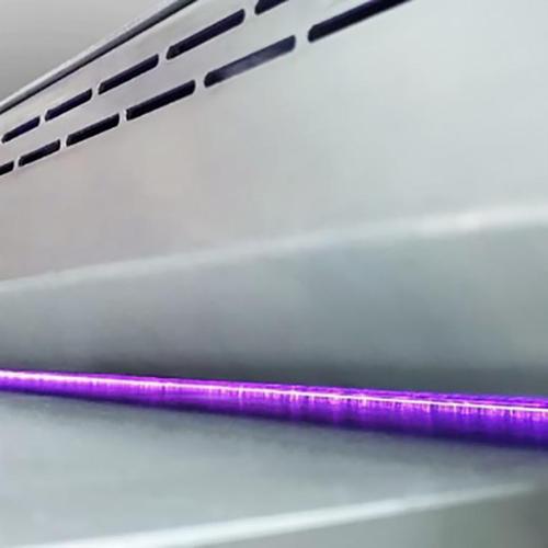
- Dielectric Barrier Discharge (DBD) Plasma Electrodes Design. Direct Plasma Design with Dual Electrode
- Electrode width can be designed based on customers' requirements
- Electrodes can be expanded with higher treatment speed
- Can be Sheet by Sheet or Reel-to-Reel treatment
- Can be standalone machine or module integrated with in-line mechanism
Atmospheric Plasma Cleaner_WaterPerformances
- Can be Single Side or Dual Side Treatment
- Reaction Gases: CDA
- Low Gas and Electricity Running Costs. Plasma Effective Width: 100 mm ~ 2300 mm. (Can be larger based on customers' requirements)
- Treatment Speed: 0.5 ~ 10 m / min in general (Can be changed based on customers' requirements)
- High Plasma Treatment Stability and Uniformity
Atmospheric Plasma Cleaner_WaterApplications/Solutions
- PCB & Substrate Technologies: Surface cleaning and modification of various PCBs (improvement of surface activation and roughness), suitable for gold/copper plating or pre-shipment treatment, FCCL (Flexible Copper Clad Laminate)
- Display & Glass Craftsmanship: Surface cleaning and modification of bare glass and ITO glass substrates (e.g., hydrophilicity improvement), cleaning for LCDs or sensors in various TP processes, glass industry
- Optics & Color Filter Processes: Various panel cleaning applications in CF processes before applying BM and R/G/B photoresists, acting as a replacement for traditional UV-Ozone cleaners to significantly save operating costs and improve cleaning efficiency
- General Materials & Film Applications: Surface cleaning and modification of various electronic or non-electronic components/materials, applicable to various metallic or non-metallic materials (e.g., PI, PET, PE, plastics, etc.), film industry, thin film growth applications